Introduction
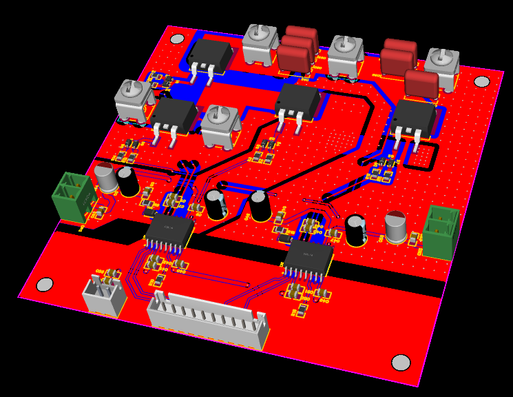
The T-type three-level half bridge (HB) is used to replace its conventional two-level HB counterparts. The Vds rating of the MOSFET switch is the same as the one in the two-level HB topology. Its main advantage is that by using a three-level topology, the voltage harmonic will be reduced, allowing for a smaller and lighter passive filter.
This board will be adopted to design a Vienna rectifier by replacing Q1 and Q4 MOSFETs with D1 and D4 Diodes.
Board description
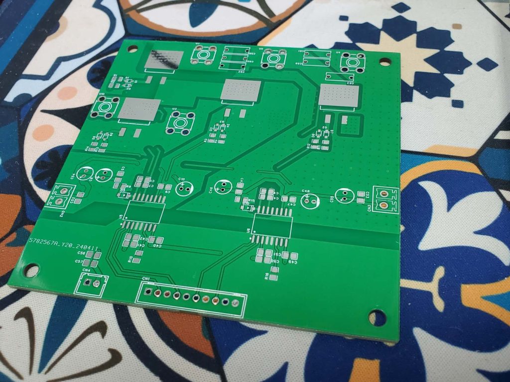
The hardware design file can be downloaded at the link: vienna_2024-05-04
Power switch
The STB24N60DM2 N-channel 600 V, 0.175 Ω, 18 A MOSFET is chosen as the switch. The MOSFET is Zener protected, which is very user-friendly for the newbie.
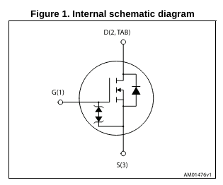
According to its datasheet, the turn-on VGS voltage should be 9V or higher.
The PWMx of the T-type consists of two pairs of complementary pulses, that is Q1=!Q3, and Q2=!Q4. For easier understanding, we can regard a T-type HB as a combination of two conventional two-level HBs (Q1-Q3 and Q2-Q4).
Isolated gate driver
Either Si8233AD or Si8233BD can serve as an isolated gate driver. These two chips are part of the popular HB driver series Si8233. These two versions are almost identical except Si8233BD has an 8V UVLO Voltage, whereas Si8233AD has a lower UVLO voltage of 5V. Without considering the power loss, these two chips can be selected according to the power supply of the gate driver. For example, if a 12V power supply is used to power the VDDA and VDDB (higher voltage side of the Si8233 chip), then both chips can be used. If a 9V power supply is used, it would be wise to choose Si8233AD, which has a lower UVLO voltage.
For one T-type HB, two Si8233 chips are required.
Power supply
A 5V power supply on the MCU side is required to power up the low voltage side of the isolation driver.
For the high voltage side, two isolated driver supplies are required. The first power supply connects to the first Si8233 chip, generating Q1 and Q3 pulses. The ground of this power supply ties to Q3s. Q1 can be considered as the high side part of the Q1-Q3 HB, therefore, a bootstrap circuit is used to supply the Q1 gate driver. The second power supply connects to another Si8233 chip, generating Q2 and Q4 pulses. The ground of this power supply ties to Q4s, which is also the ground of the high voltage side. Similarly, the gate driver supply of Q2 is provided by a bootstrap circuit.
DC-link capacitor
We limit our board size to 10cm * 10cm to lower the manufacturing cost in JLC. Therefore, a DC-link capacitor is not included on this board, which will be connected from a separate capacitor bank board cap_3Level_2024-05-04. Nevertheless, we provide several CBB capacitors at the DC-link to avoid potential ringing.
Test
The test procedure is similar to the one presented in https://bluespider.top/index.php/2024/05/03/600vdc-30a-three-phase-inverter-v1-0-cihangir-for-lab-experimental-part-i-solder-and-initial-test/.
The key part is to ensure that Q1-Q3 and Q2-Q4 are properly complementary with enough dead-time, in order to avoid a shoot-through event.